Creating a Low Power LED DCF77 Clock: A DIY Project Journey
During a visit to the local hackerspace, I observed someone engraving signatures onto a silicon wafer as a retirement gift, sparking an idea. With a colleague nearing retirement, I sought silicon wafers on eBay and was fortunate to find some. What began as a simple notion soon evolved into a larger project: constructing a clock with a silicon wafer serving as the clock face, complete with LEDs—the epitome of any “cool” project.
In Germany, radio-controlled clocks powered by the DCF77 radio protocol are common. DIY enthusiasts can find analog clock modules equipped with several exposed test pads. I initially assumed that one of these pads might carry the demodulated radio signal necessary for decoding a DCF77 timestamp. Upon receiving a clock module from Amazon, I began probing for signals to synchronize the LEDs with the analog clock.
Unfortunately, the DCF77 signal wasn’t readily accessible on the exposed pads. However, further exploration beneath the housing revealed promising labeled pads. Upon probing these additional points, I confirmed they indeed carried the required signals. With thin wires, I easily routed these signals to the contact pads outside the housing.
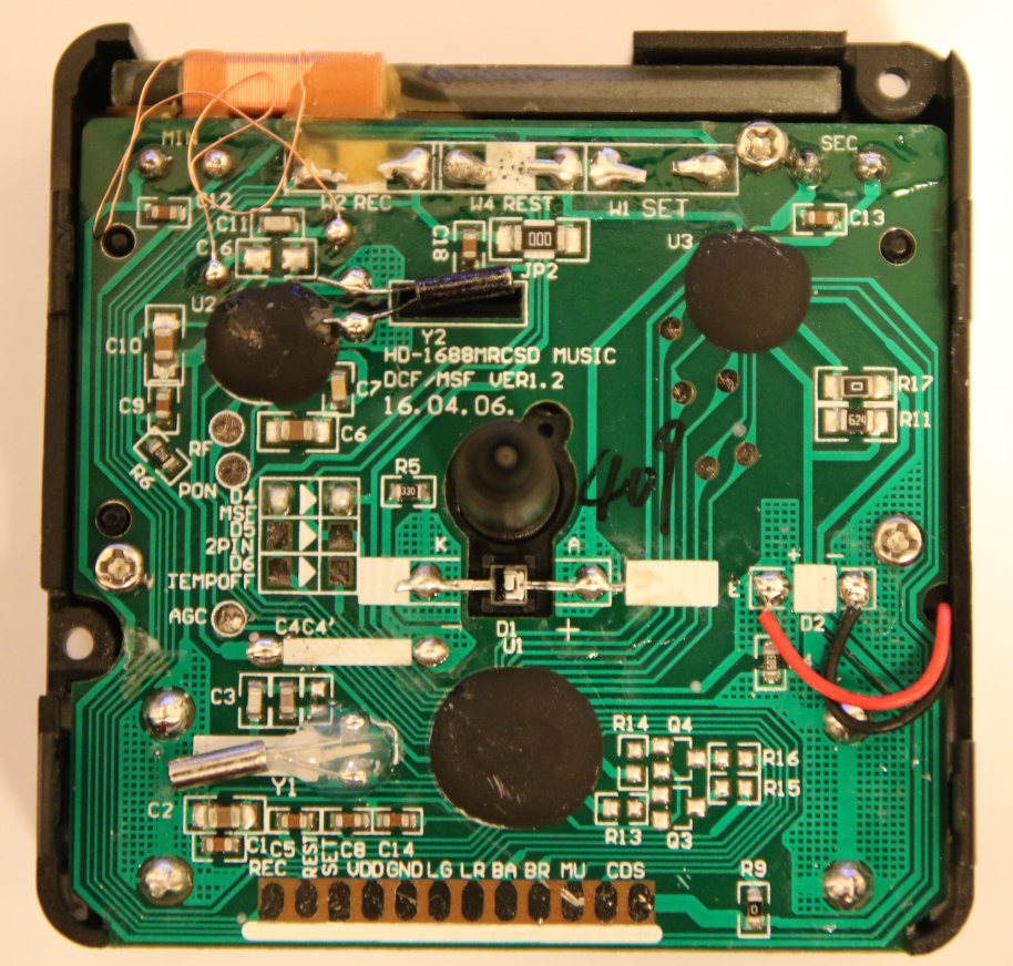
The clock module operates on a single AA battery, with digital signal logic levels ranging from 1.2V to 1.5V. After initial oscilloscope testing, I soldered wires and connected them to a Cypress FX2 logic analyzer, compatible with Sigrok. Adjusting logic levels required applying a bias voltage to the ground, with 0.7V proving just enough.
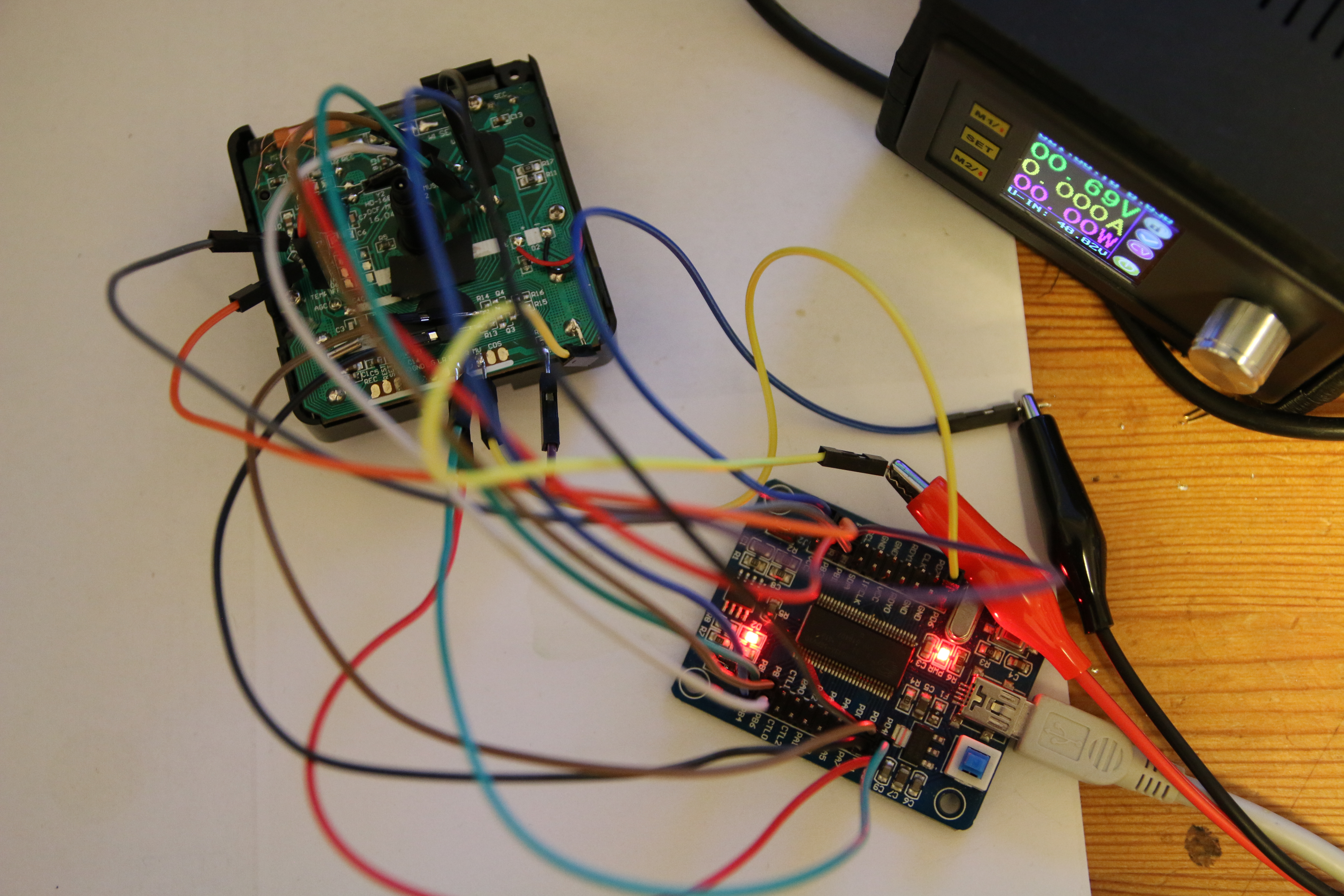
PulseView records every sample directly into RAM, making long-term measurements memory-intensive. To address this, the Sigrok command line tool writes measurements into VCD files, conserving memory by recording data only when signal levels change. VCD files are compatible with various viewer programs.
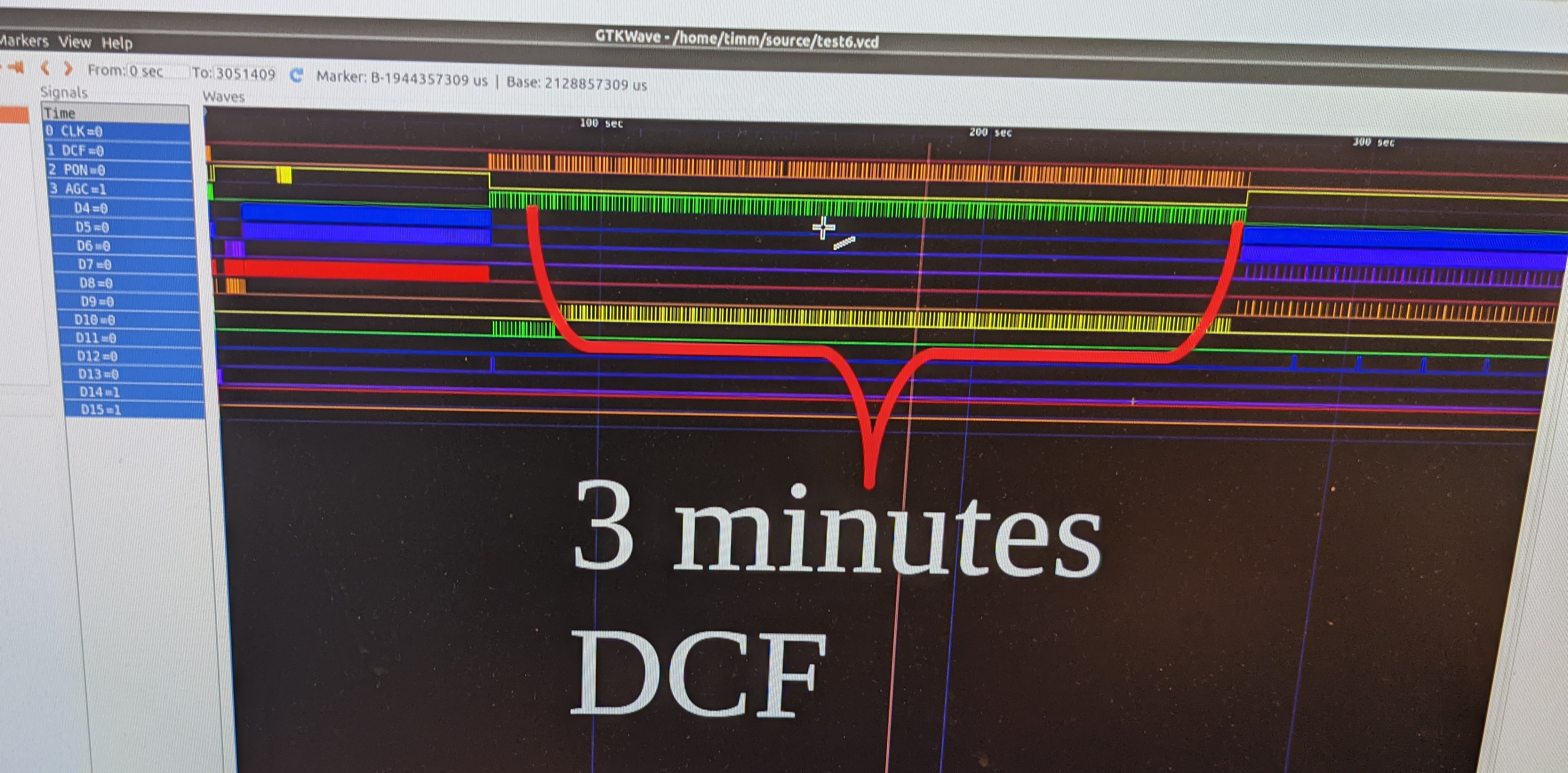
Extended measurements revealed the radio receiver activates every three hours, with a three-minute demodulated signal duration—sufficient for decoding a timestamp. This allows for frequent LED driver clock synchronization, even with less than 100% precision.
With these findings, plans expanded. Armed with a clock module powered by a single AA battery and knowledge of the demodulated radio signal’s location, I envisioned powering the LEDs with the same battery. This led me to research electronic components meeting my requirements: a low-power boost converter for LED and logic supply conversion and a low-power microcontroller for implementing the logic.
My choice was:
- Boost converter TPS610986: Low power boost converter with 3.3V output voltage and minimum 0.7V input voltage.
- Microcontroller STM32G031: ST just started the new STM32G series microcontroller. These microcontrollers were further optimized for low power usage and have the newest revision of peripherals, which allow low power operation. The Cortex-M0+ core is very power efficient.
- Addressable LEDs WS2812B: The WS2812B are very commonly used addressable RGB Leds. The color of each LED can be set via one data line. The LEDs are functioning as a shift register. Data is shifted to the next LED in the row when data is continuously streamed via the data pin. The datasheet says, that the operating voltage is from 3.5V to 5.3V, but in my case worked fine at 3.3V.
- Level shifter from 1.5V to 3.3V signals: simple grounded emitter transistor circuit. The signal level from the clock module is 0V when idle. So no current is flowing on idle.
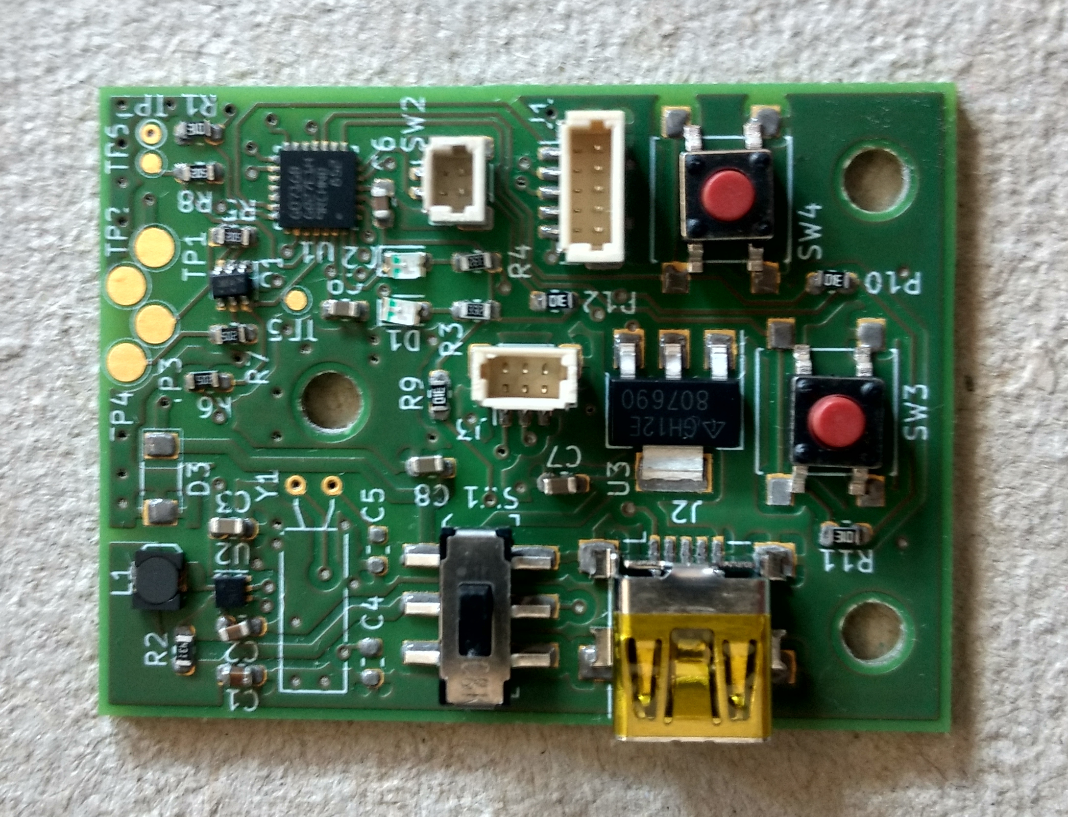
With components selected, I created a schematic in KiCAD and designed the PCB with compactness in mind, utilizing mostly SMD parts. SMD resistors with 0603 size are small but are still easy to hand solder. To aid in dispensing the solder paste, I ordered a laser-cut solder paste stencil.
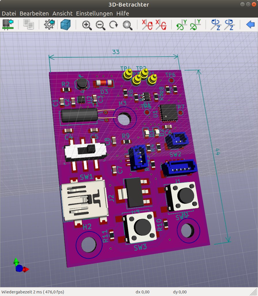
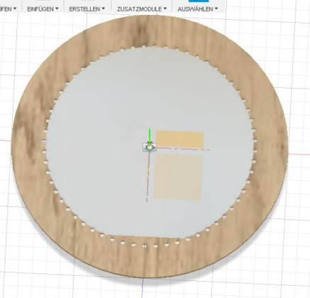
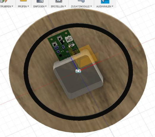
Kicad can export a 3D Model of the assembled PCB, which can then be loaded into Fusion360. I discovered a ready-to-use model of the DCF77 clock module on GrabCAD. Using this, I meticulously modeled the entire clock housing to ensure everything fit seamlessly.
| Front | Back |
|---|---|
 |
 |
While I waited for the electronic components and PCBs to arrive, I started with the firmware in parallel. The firmware is written from scratch in C++. My goal was to try to design the firmware object-oriented. A small operating system and even the peripheral drivers were written in C++. The peripheral drivers are implemented on top of the STM’s Low-Level peripheral abstraction layer, which allows to use of the peripherals with very low overhead. A low amount of firmware instructions will help in lower execution times and therefore less energy to be consumed.
To save energy clever use of the STM32G0 power-saving features is necessary. The STM32G0 uses the most energy while the CPU is fully running and all needed peripherals are turned on. The CPU doesn’t need to run all the time. Most of the time it is waiting for the next event. So setting the CPU into sleep mode, while nothing has to be computed, is very handy. Peripherals will quickly wake up the CPU from sleep mode by hardware interrupts. To save even more energy, the CPU can be set into stop mode. In stop mode the core will lose the content of the RAM and the execution of the program will start from the very first instruction, after the processor was woken up. In stop mode, only a few peripherals are still in operating mode, in our case the RTC, the RTC backup memory, and digital inputs for wakeup signals. Because the content of the RAM gets lost in stop mode, the RTC backup memory has to be utilized for storing permanent data.
With the firmware I tried out some concepts, I first figured out in my mind. The operating system should handle tasks event-based. The operating system is also used to create a barrier between hardware and logic implementation. Peripherals will trigger a hardware interrupt routine, which only does short handling of status flags and will trigger the os to put an event into a fifo. After that, the scheduler will take over and notify each task, which has registered for that event type. The logic is implemented as tasks. For example, decoding the DCF frame is a task, and driving the LEDs is a task. Each task can register its observable events. Multiple tasks can register for the same event, so multiple tasks will be notified of that specific event. Each task has its state (wake, sleep, deep sleep). The operating system will only go into sleep or stop mode if all tasks are corresponding. The operating state of peripherals is handled by the operating system, too. Peripherals will only go into operating mode if they are requested so. And peripherals will be powered down if no task needs it anymore. That allows the lowest amount of energy to be used for the specific use case.
Manufacturing the PCB was quite fun. This was my first project in which I tried to reflow the assembled PCB. The solder paste was applied with an old credit card for extra style.
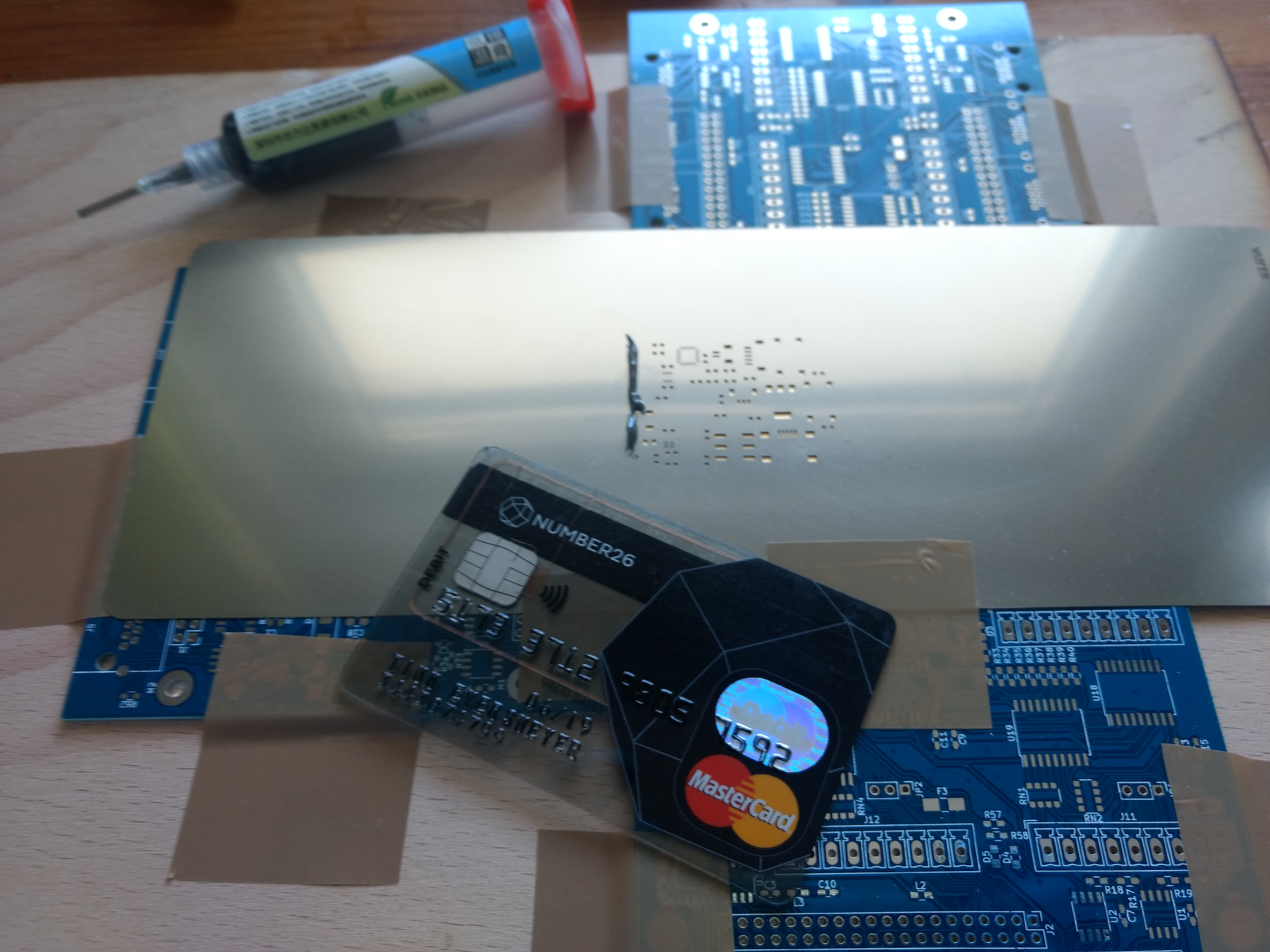
With some practice I got a working result. It is important to have the stencil snug on the PCB. The cutouts shall be in the right place on the pads. With too much solder paste or too much pressure, the solder paste gets squished between the stencil and PCB.
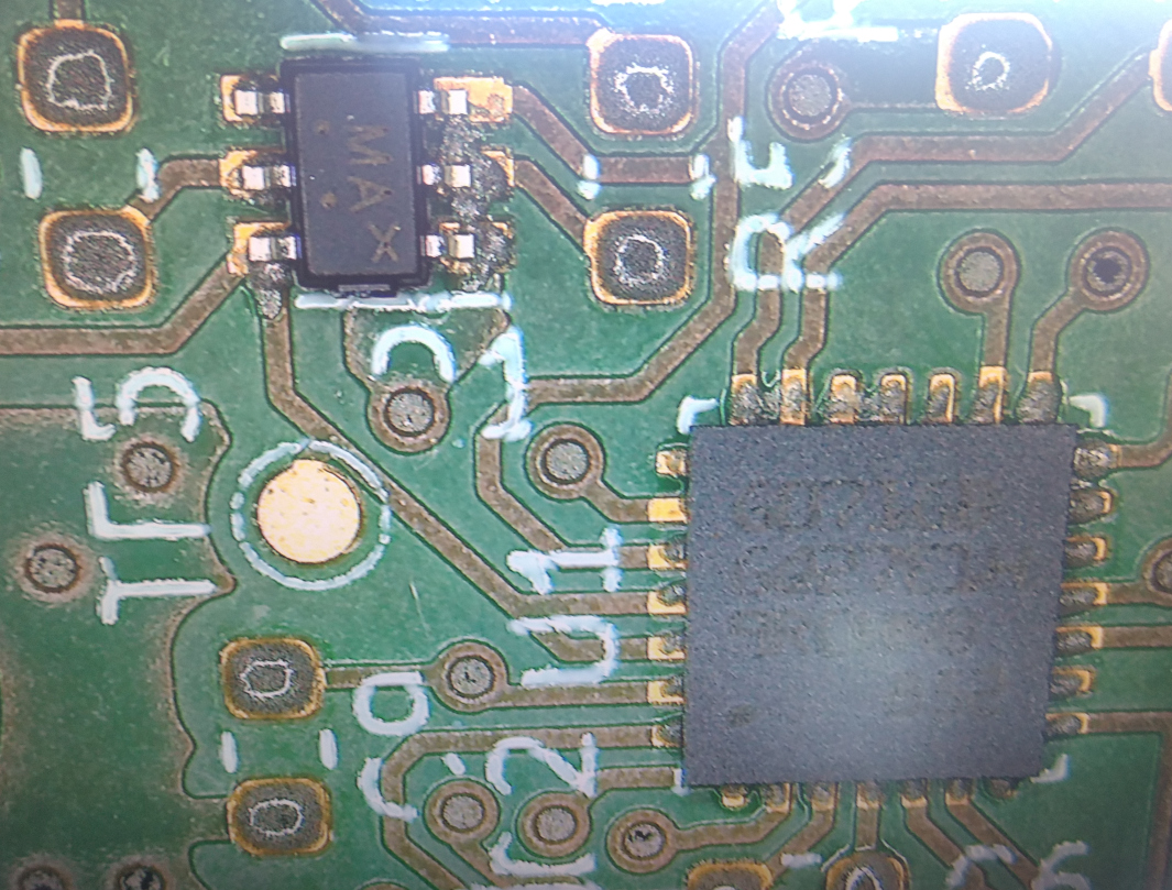
I placed components with sharp tweezers by hand. Reflow soldering was done via a hot air station. I have no hot plate, but the low-temperature solder paste just worked fine with only hot air.
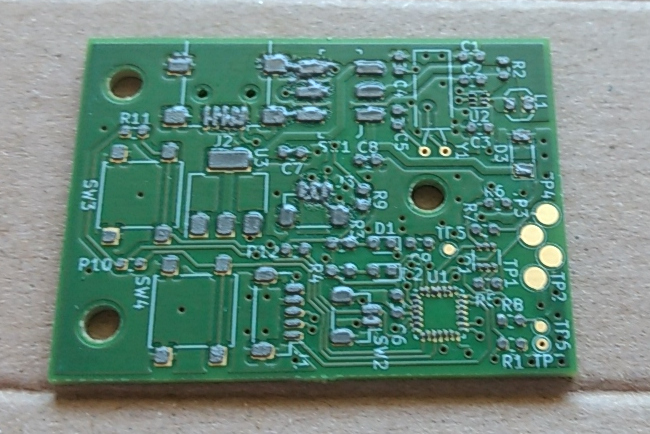
Before soldering the placement is checked under a microscope.
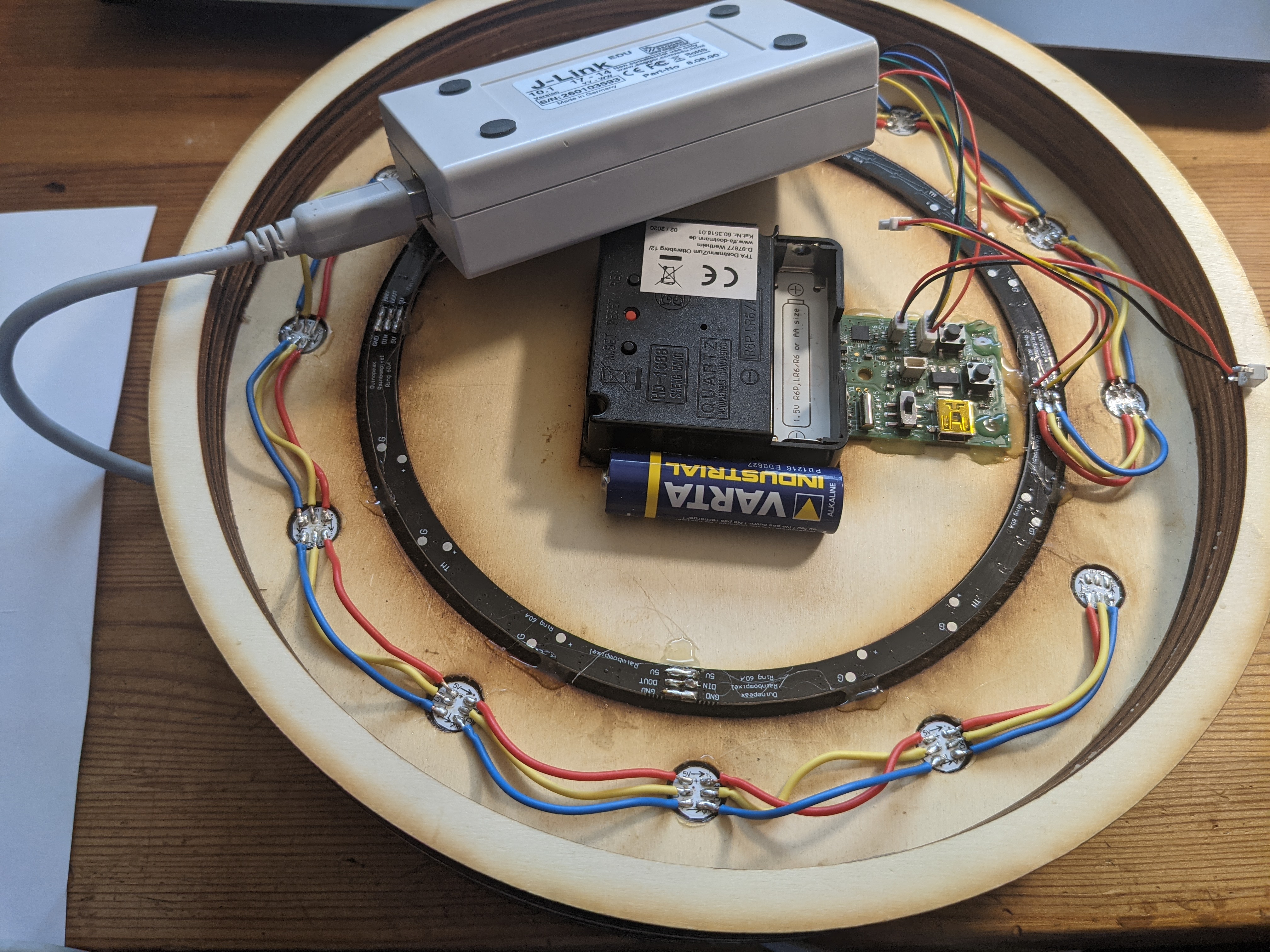
The LEDs and PCB are glued with hot glue into the housing. Everything is wired up and the debugger probe is plugged in.
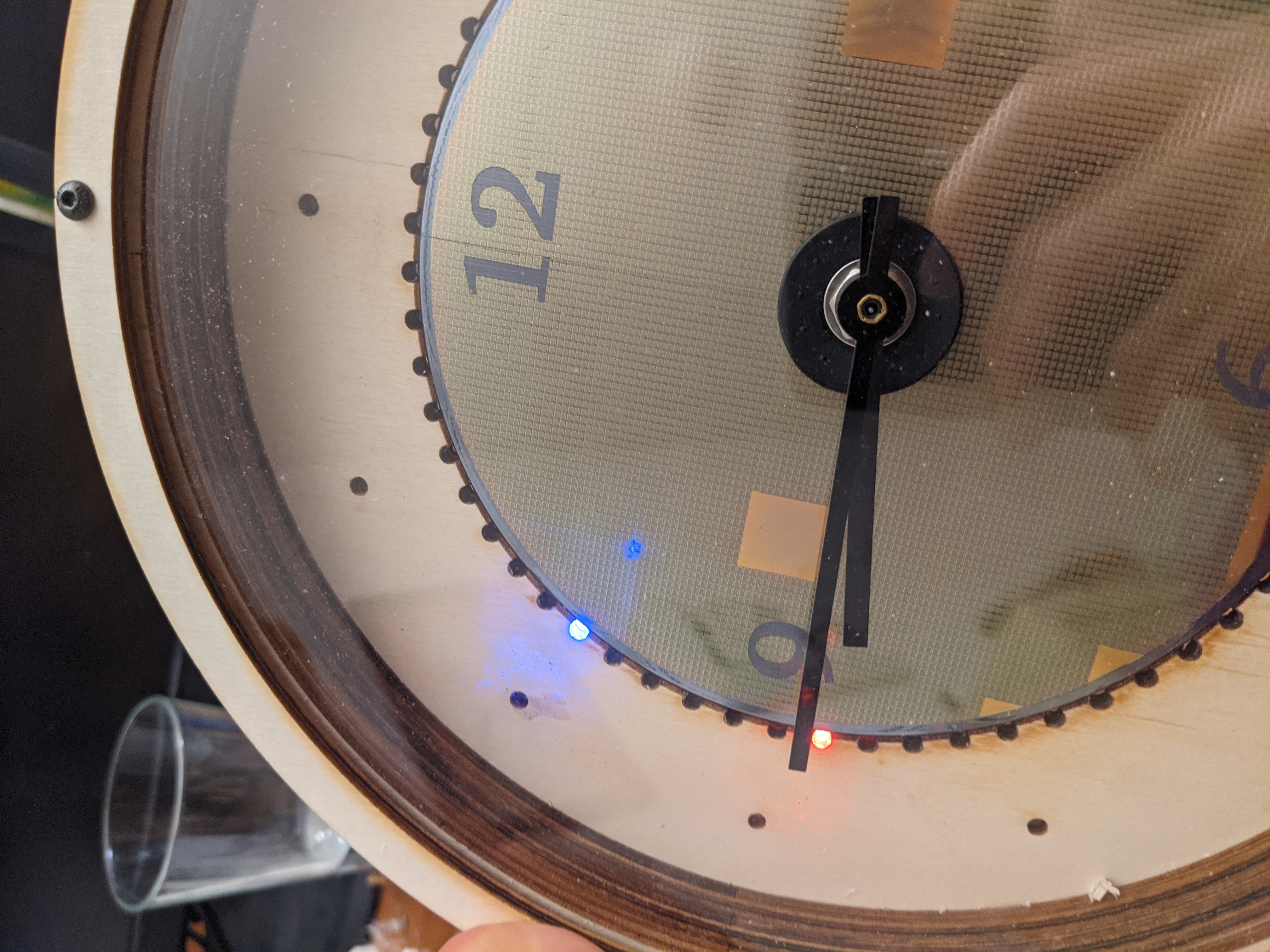
After several hours of coding and debugging, I had a first working version. The blue light indicates seconds and the red light stands for minutes.
Github firmware: https://github.com/saeugetier/LedDcfClock Github hardware: https://github.com/saeugetier/LedDcfClockHardware